


CEO Message
Greetings, I am Hong Jin-pyo, CEO of JP SCIENCE.
Since our establishment in 2024, JP SCIENCE has been pursuing continuous research and innovation in the field of advanced scientific technology. Our goal is to contribute to industrial development by providing customers with the highest quality services and products.
Based on expertise and trust, we always strive to provide optimal solutions that meet our customers' needs. JP SCIENCE will continue to grow as a competitive company in the global market by introducing innovative technologies through continuous research and development.
Sincerely, Hong Jin-pyo
R&D Timeline
JP SCIENCE's Innovative Research Journey
2023
Research on defect control-based single cell selection memory dual-function selector-only memory device core technology (Feb 2023 ~ Jan 2026)
Development of high-speed/low-power/high-reliability 2-terminal field-free SOT-MRAM core technology and IP acquisition (Apr 2023 ~ Dec 2027)
2021
Multi-level brain function mimicking device using magnetic skyrmions (Apr 2021 ~ Dec 2023)
Research on high-stretchability energy harvesting anode materials and properties core technology for self-charging implantable medical devices (Mar 2021 ~ Feb 2024)
2019
Large-area/integrable complementary SOT-MTJ structure-based ultra-low power unit cell reconfigurable spin logic device core technology (Jun 2019 ~ Dec 2021)
2017
Research on 3D stacked cross-bar vertical spin-torque magnetoresistive memory integration and application technology (Mar 2017 ~ Feb 2020)
2016
Research on 1D fiber-based energy harvesting clothing operated by human body movement (Dec 2016 ~ Nov 2017)
Forming-free a-C:Ox based ReRAM core technology development (Oct 2016 ~ Sep 2021)
Development of neuron device and system core technology mimicking nerve cells using nanoelectronic device technology (Aug 2016 ~ Jul 2021)
Services
JP SCIENCE's Professional Services
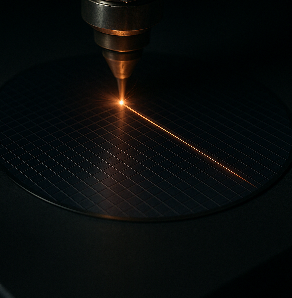
Thin Film Deposition
We provide high-quality thin film deposition services using state-of-the-art equipment. Applicable to various fields including semiconductors, displays, and optical devices.
HR-XRD Measurement & Analysis
We precisely measure and analyze material crystal structure, thickness, and composition through high-resolution X-ray diffraction analysis. We provide optimal solutions based on accurate data.
Ion Milling
We provide precision processing services using ion milling technology. Nano-level precision surface treatment and micro-processing of various materials are possible.
Products
JP SCIENCE's Innovative Products

Insulation Bonding Wire
JP SCIENCE's flagship product, Insulation Bonding Wire, is a high-performance wire used in semiconductor packaging processes. It features excellent insulation properties and durability, optimized for high-density semiconductor products.
- Excellent insulation properties
- High heat resistance and durability
- Fine pitch application capability
- Custom manufacturing in various sizes and specifications
Technology
JP SCIENCE's Core Technology and Research Achievements
Patents
Research Papers
Corporate Partnerships
Research Fields
Semiconductor Materials
We research high-performance semiconductor manufacturing technology through next-generation semiconductor material development and characterization analysis.
Nanotechnology
We develop nano-scale material and structure control technologies and apply them to various industrial fields.
Measurement & Analysis
We provide precise data collection and interpretation using advanced measurement equipment and analysis technology.
Contact Us
If you have any questions about JP SCIENCE, please feel free to contact us anytime.
Address
Room 428, Natural Science Building, Hanyang University, 222 Wangsimni-ro, Seongdong-gu, Seoul, South Korea
Phone
+82-2-2220-0911
info@jpscience.co.kr